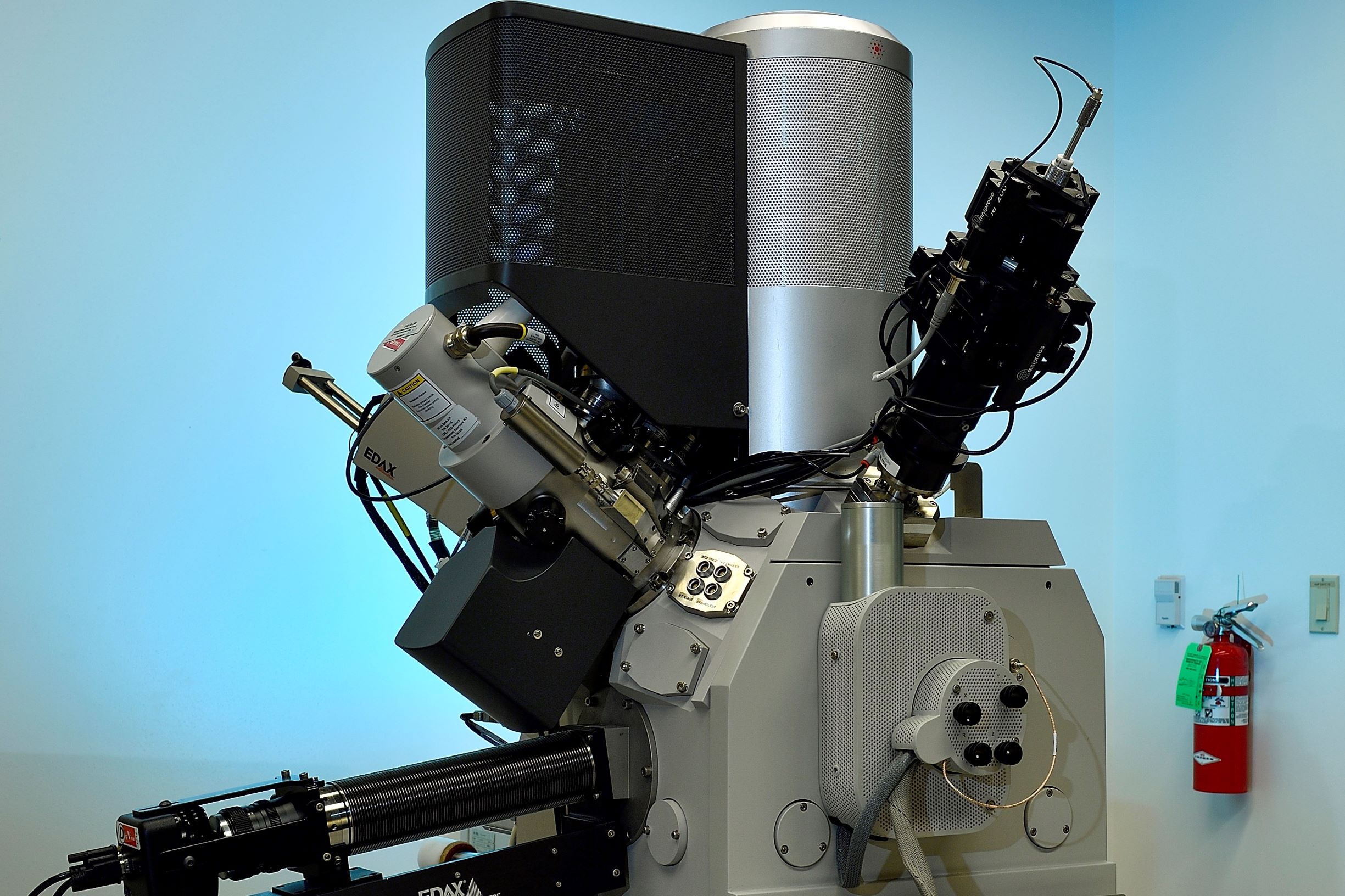
 The FEI Nova 200 NanoLab (a dual column ultra-high resolution field emission scanning
electron microscope (SEM) and focused ion beam (FIB)) was installed in January 2005.
The FEI Nova 200 NanoLab (a dual column ultra-high resolution field emission scanning
electron microscope (SEM) and focused ion beam (FIB)) was installed in January 2005.
Etching with an accelerated Ga ion beam and deposition using Pt are available for nanoscale prototyping, machining, 2-D and 3-D characterization, and analysis.
The system is expandable making additional gas injection systems available for deposition and etching in the future. Nanoscale chemical analysis may be performed with an EDAX energy dispersive X-ray spectroscopy (EDS) system with spectrum imaging control. The secondary electron image resolution at the dual beam coincidence point is 1.5 nm at 15 kV. The FIB optics have better than 7 nm resolution at 30 kV.
A high resolution digital patterning system controlled from the User Interface is also available. Predefined device structures in Bitmap format can be directly imported to the patterning system for nanoscale fabrication. The FEI Nova 200 is also equipped with an Omniprobe Autoprobe nano-manipulator, with 10 nm positioning resolution.
The manipulator can be fit with either sharp whisker probes for electrically probing samples or standard probes for mechanical testing. Additionally, the manipulator allows for extraction of a milled, site-specific region for transmission electron microscopy examination.
The instrument is also outfitted with an electron backscattered diffraction (EBSD) system, which allows for crystallographic determination on the nanoscale, and, along with imaging capabilities, 3-D reconstructions of the material and crystallography.
Instrument Specifications
Electron Optics
|
Detectors
|
|
Fabrication and Machining
|
|
Ion Optics
|
Equipped with:
|
|
Gas Chemistry
|