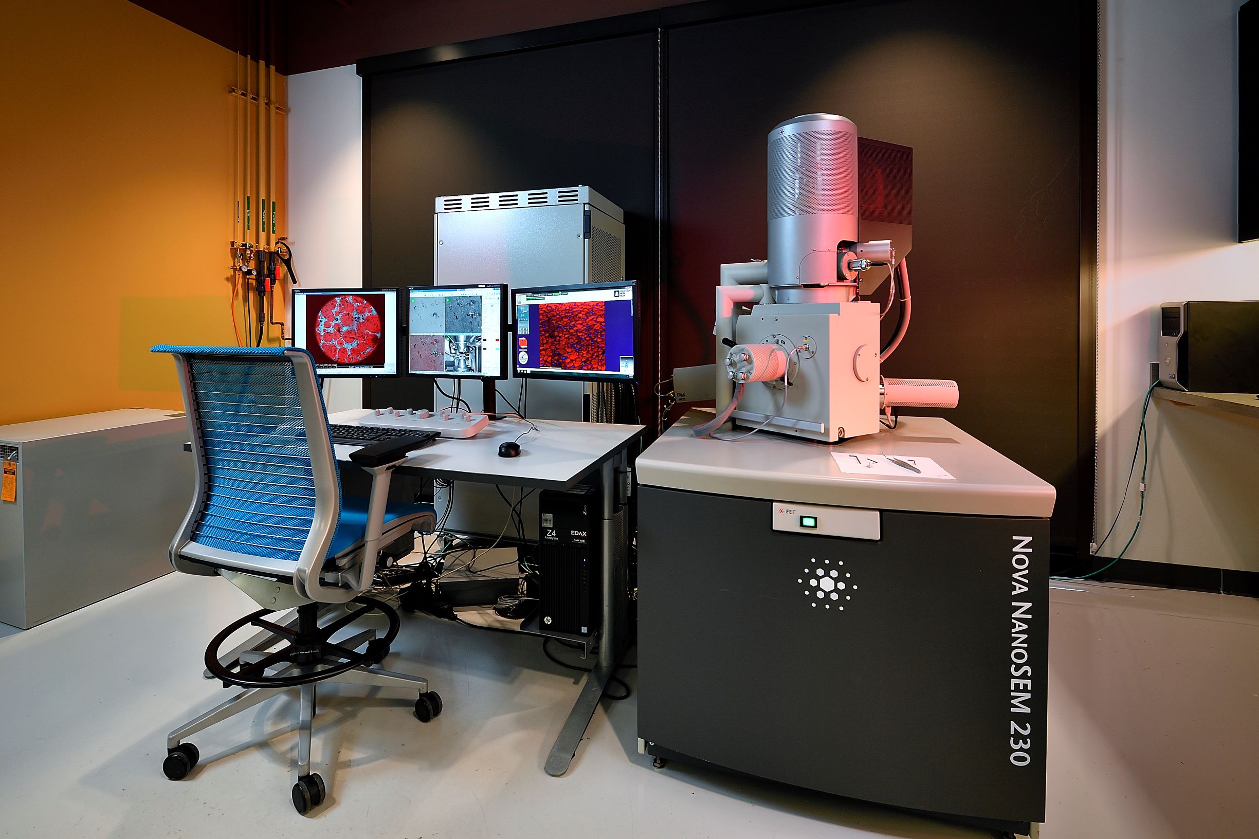
 The FEI Nova NanoSEM 230 was installed in December 2009.
The system is equipped with an EDAX Apollo X silicon drift detector energy dispersive X-ray spectroscopy (EDS) system.
The instrument is also outfitted with an electron backscattered diffraction (EBSD) system, which allows for crystallographic determination on the nanoscale, and, along with imaging capabilities, 3-D reconstructions of the material and crystallography.
Instrument Specifications
|
Electron Optics • High resolution field emission-SEM column, with: • Resolution @ optimum WD (high vacuum) • Beam landing energy: 50 V - 30 kV • Probe current: 0.6 pA - 100 nA continuously adjustable |
Detectors • In-lens SE detector (TLD-SE) |
|
Equipped with: • EDAX Apollo X Silicon Drift Detector (SDD), Genesis software • TSL Digiview III Electron Backscatter Diffraction (EBSD) detector, OIM™ software |