Usage Rates for Internal, External Non-Profit, and Commercial Users
All rates listed are hourly unless otherwise stated and are applied in 1-minute increments.
Electron and Ion Microscopy
| Instrument | Capabilities | Operation Modes | |
|---|---|---|---|
|
|
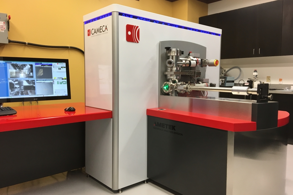
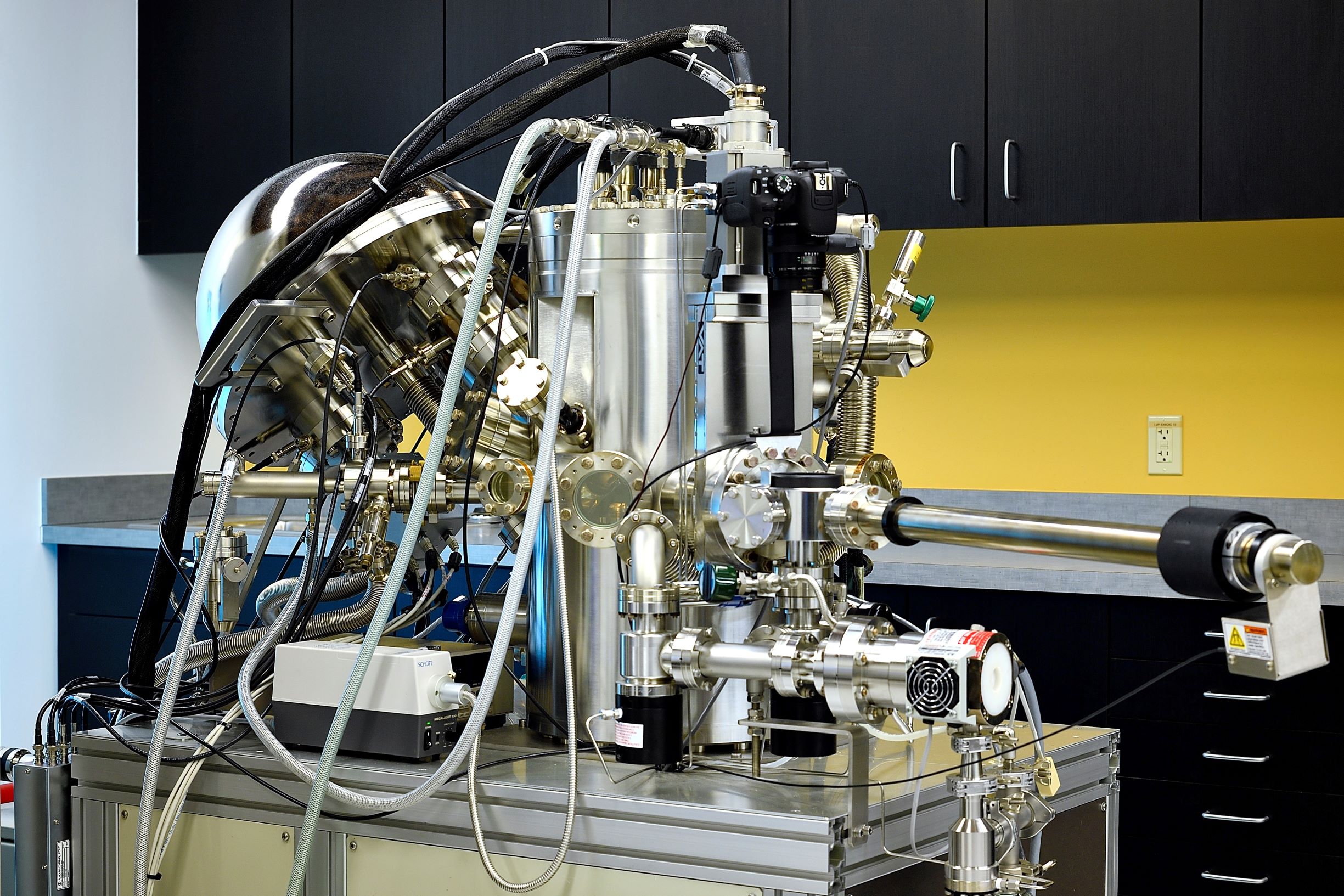
3D Atom Probe Microscope Cameca LEAP 5000XS HR Atom Probe Microscope Room: E-178B |
Analysis of Metals, Semiconductors and Insulators 3D Atom Scale Elemental Analysis 3D Atom Scale Crystal Structure Analysis 3D Analysis of Interfaces |
Voltage Pulsed APT Laser Pulsed APT Field Ion Microscopy |
|
|
High-Resolution Analytical TEM TS Talos F200X G2 S/TEM Room: E-178E |
2D/3D Structural Imaging Crystal Structure Analysis Elemental Analysis/Imaging |
BF, DF, EDS, BF/DF/HAADF STEM, 4D STEM, Tomography |
|
|
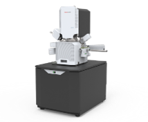
DualBeam FIB/SEM TS Helios 5 PFIB Cxe Room: E-178D |
2D/3D Imaging Micro-machining & Deposition Site Specific Sample Preparation 2D/3D Elemental + Crystal Structure Analysis/Imaging |
SE/BSE/SI, High-resolution SE/BSE Ga FIB, Pt GIS Nanomanipulator, Pt GIS, EBSD, EDS |
|
|
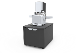
Analytical FEG-SEM TS Apreo 2 S LoVac Room: E-178P |
2D Imaging 2D Elemental Analysis/Imaging 2D Crystal Structure Analysis/Imaging |
SE/BSE, High-resolution SE/BSE EDS EBSD |
|
|
Environmental SEM (ESEM) TS Quattro S ESEM Room: E-178E |
2D Imaging 2D Elemental Analysis Low pressure |
SE, BSE EDS SE, BSE, EDS |
|
|
Analytical TEM |
2D/3D Structural Imaging Crystal Structure Analysis Elemental Analysis/Imaging |
BF, DF, SAED, EDS, STEM BF/DF/HAADF, OIM-PED |


Surface & Thin Film Analysis
| Instrument | Capabilities | Operation Modes | |
|---|---|---|---|
|
|
XPS Imaging Spectrometer PHI 5000 Versaprobe Scanning XPS Microprobe with UPS Room: E-178E |
UHV compatible materials Chemical Bond State Surface Spectroscopy Work Function measurements Compositional Depth Profiling |
XPS, ARXPS UPS Ar Ion Sputter Gun Five axis motorized stage |
|
|
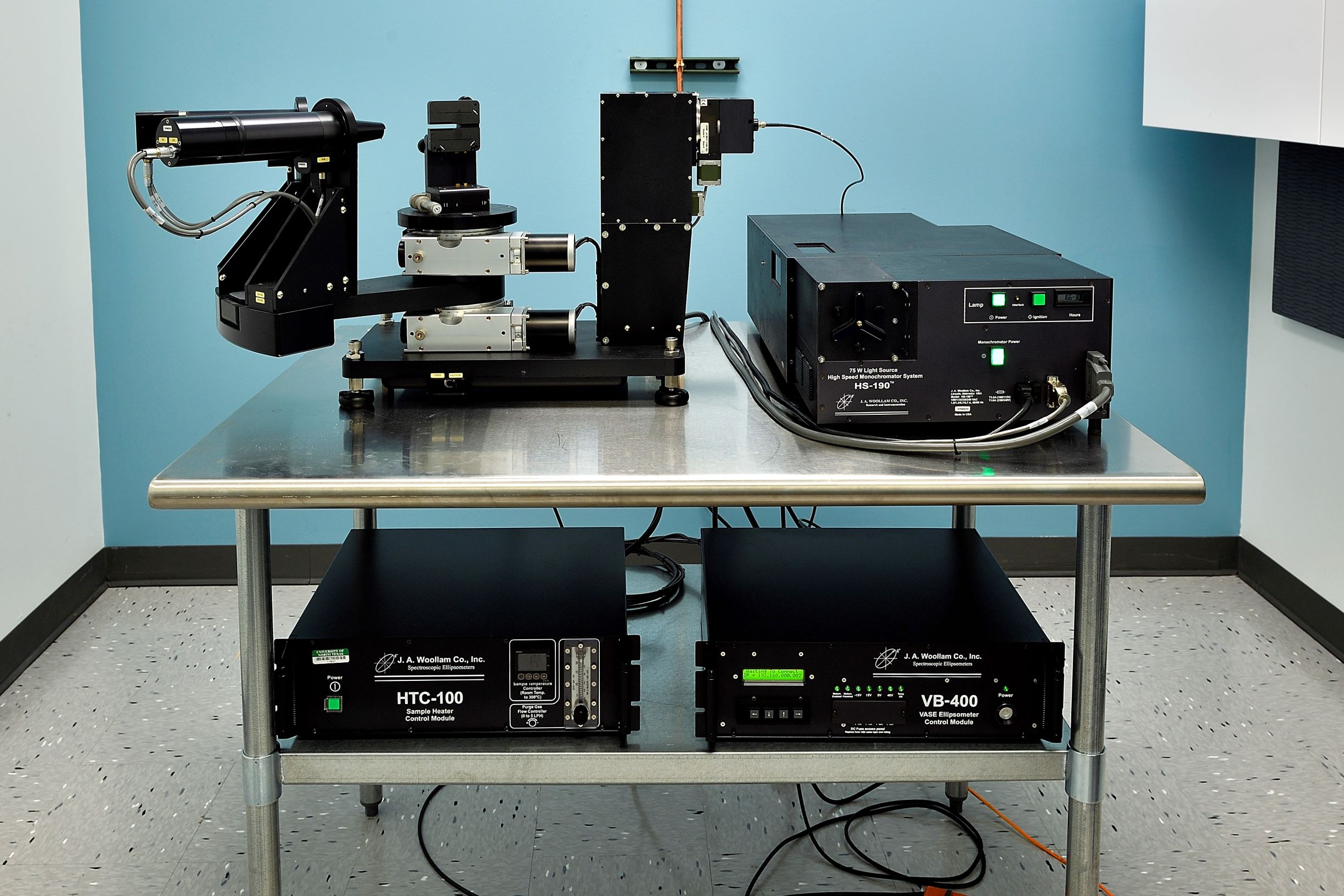
Spectroscopic Ellipsometer J.A. Woollam Variable Angle Spectroscopic Ellipsometer Room: E-178K |
characterize surfaces, thin films, and microstructure determine optical constants determine film thicknesses determine doping concentration |
250nm to 2200nm spectral range Heating Stage
|
|
|
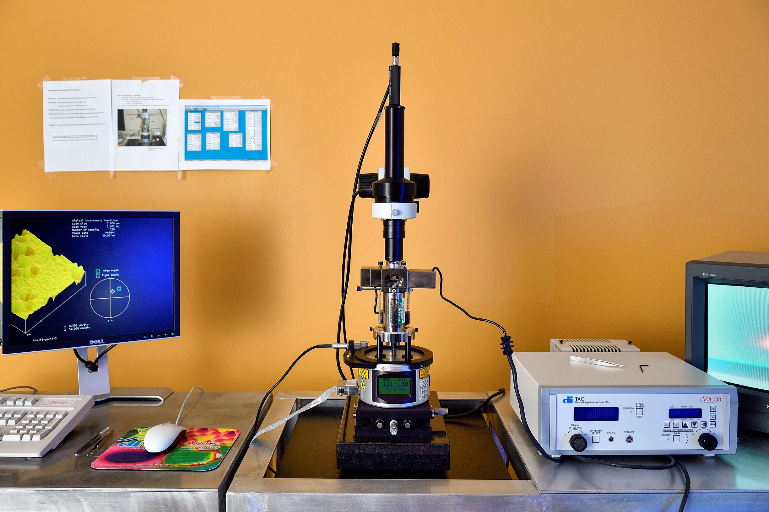
Scanning Probe Microscope Veeco Multimode Nanoscope III SPM Room: E-178M |
AFM, STM, MFM, SCM | |
|
|
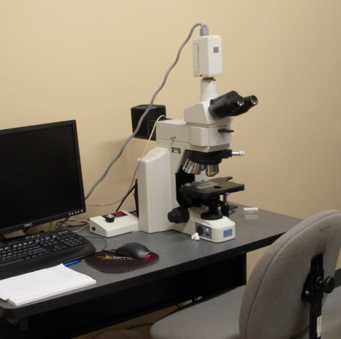
Optical Microscope Nikon Eclipse ME600 Digital Optical Microscope Room: E-178K |
Sample Preparation
| Instrument | Capabilities | Operation Modes | |
|---|---|---|---|
|
|
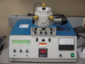
SEM Ion Etching & HR Coating Gatan 682 Precision Etching Coating System Room: E-178K |
Previously Managed Instruments
|
|
FEI Quanta 200 ESEMRETIRED, REPLACED BY TS QUATTRO S ESEM] |
|
|
FEI Nova 200 NanoLab FIB/SEM[RETIRED, REPLACED BY TS Helios 5 PFIB Cxe] |
|
|
FEI Nova NanoSEM 230[RETIRED, REPLACED BY TS Apero 2 s LoVac] |
|
|
Rigaku Ultima III XRD[RETIRED] |
|
|
Imago LEAP 300X HR [RETIRED, REPLACED BY CAMECA LEAP 5000XS] |
|
|
Philips EM420 120keV TEM [CURRENTLY MANAGED BY MTSE] |
|
|
PHI 670xi Scanning Auger Nanoprobe [RETIRED] |
|
|
Nicolet Almega XR Dispersive Raman spectrometer [RETIRED] |
|
|
Nicolet 6700 Fourier Transform Infrared Spectrometer (FTIR) [RETIRED] |
|
|
Skyscan 1172 High Resolution µ-CT 3D Imaging System [RETIRED] |
|
|
Gatan 691 Precision Ion Polishing System [RETIRED] |


